
 Researchers of the American IBM for the first time, successfully transmitted a short radio signal (the three letters of their company name) to a pioneering receiver chip, containing transistors made from the new "miraculous" material, the graphene. The achievement, albeit at an early stage, paves the way for a future revolution in wireless communications.
Graphene, one of the finest electronic nano-materials, is promising in a wide range of practical applications, from flexible displays to fast integrated circuits. Until now, wireless circuits, like those contained in the devices Bluetooth and Wi-Fi, could not be made with graphene transistors, because it is technically difficult - because graphene is easily damaged - to combine in the same "chip" the sensitive graphene transistors with the other necessary metal components of a circuit, such as resistors and coils.
This difficulty, however, has now been overcome by simply reversing the usual production process, namely first putting the metal elements on the chip and then the transistors. Researchers at IBM's Watson Research Center in New York, published in the journal Nature Communications, according to New Scientist, have announced that they have created the world's most advanced and fully functional integrated chip. from graphene, which has 10.000 times better performance than any other related effort in the past.
Such chips can in the future make wireless devices (tablets, smart phones, etc.) much faster - but also cheaper - while giving them new possibilities, which are not possible with today's silicon chips. The researchers point to the possibility of seamless integration of graphene chips into existing silicon-based electronic technology, as the graphene chip "steps" onto a conventional silicon wafer, so the existing production lines of chip manufacturing industries will not need to be significantly modified. .
The graphene, discovered about a decade ago (and awarded a Nobel to its creators), consists of flat carbon sheets of only one individual thickness, each placed in a hexagonal arrangement that resembles a hive. The new material has unusual electrical, optical, thermal and mechanical properties that make it suitable for wireless communications.
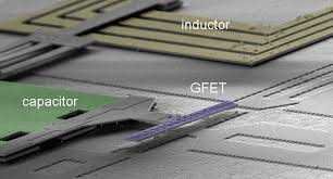
The signal "I-B-M" (digital text of three letters) was broadcast on the radiofrequency των 4,3 GHz χωρίς καμία απώλεια ή παραμόρφωση. Το ολοκληρωμένο κύκλωμα αποτελείται από τρία τρανζίστορ γραφενίου, τέσσερα επαγωγικά πηνία, two capacitors and two resistors. All these components of the "chip" are located in an area of 0,6 square millimeters. In addition, thanks to the high conductivity of graphene as a material, the new circuit uses less electricity than conventional radio chips.
Η research της ΙΒΜ χρηματοδοτήθηκε από την πανταχού παρούσα Υπηρεσία Προωθημένων Αμυντικών Ερευνών (DARPA) του Πενταγώνου των ΗΠΑ, τον φορέα που ουσιαστικά ξεκίνησε τη δημιουργία του Ίντερνετ και «βλέπει» παντού δυνητικές στρατιωτικές applications.
However, according to estimates by other (competitors) researchers, although the new achievement is indeed impressive, it will take at least 20 years until these "hybrid" graphene-silicon chips are adopted on a massive scale.