
 Researchers of the American IBM managed for the first time to successfully transmit a short radio signal (the three letters of their company name) to a pioneering chip-receiver, which contained transistors made by the new "miracle" material, the graphene. The achievement, albeit at an early stage, paves the way for a future revolution in wireless communications.
Graphene, one of the finest electronic nano-materials, is promising in a wide range of practical applications, from flexible displays to fast integrated circuits. Until now, wireless circuits, like those contained in the devices Bluetooth and Wi-Fi, could not be made with graphene transistors, because it is technically difficult - because graphene is easily damaged - to combine in the same "chip" the sensitive graphene transistors with the other necessary metal components of a circuit, such as resistors and coils.
This difficulty, however, has now been overcome by simply reversing the usual production process, namely first putting the metal elements on the chip and then the transistors. So, the researchers of the IBM Watson Research Center in New York, who made the relevant publication in the journal "Nature Communications", according to "New Scientist", announced that they have created the world's most advanced and fully functional integrated circuit (chip) from graphene, which has a performance 10.000 times better than any other related effort in the past.
In the future, such chips can make wireless devices (tablets, smart phones etc) much quicker - but cheaper - giving them new features that are not possible with today's silicon chips. Researchers point to the possibility of smoothly integrating graphene chips into existing silicon-based electronics, as the graphene chip is pressed onto a conventional silicon disk, so the existing chip production lines will not need to be significantly modified .
The graphene, discovered about a decade ago (and awarded a Nobel to its creators), consists of flat carbon sheets of only one individual thickness, each placed in a hexagonal arrangement that resembles a hive. The new material has unusual electrical, optical, thermal and mechanical properties that make it suitable for wireless communications.
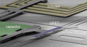
The "I-B-M" signal (three-letter digital text) was transmitted to the 4,3 GHz radio frequency without any loss or distortion. The integrated circuit consists of three graphene transistors, four inductors, two capacitors and two resistors. All of these "chip" components are located in an area of 0,6 square millimeters. Moreover, thanks to the high conductivity of graphene as a material, the new circuit uses less electricity than conventional radio chips.
The IBM survey was funded by the ubiquitous US Pentagon of Advanced Defense Research (DARPA), the body that has begun creating the Internet and "sees" everywhere potential military applications.
However, according to estimates by other (competitors) researchers, although the new achievement is indeed impressive, it will take at least 20 years until these "hybrid" graphene-silicon chips are adopted on a massive scale.